Thin-Film Photovoltaic Engineering Market Report 2025: In-Depth Analysis of Growth Drivers, Technology Innovations, and Global Opportunities. Explore Key Trends, Forecasts, and Strategic Insights Shaping the Industry.
- Executive Summary and Market Overview
- Key Technology Trends in Thin-Film Photovoltaics
- Competitive Landscape and Leading Players
- Market Growth Forecasts (2025–2030): CAGR, Revenue, and Volume Analysis
- Regional Market Analysis: North America, Europe, Asia-Pacific, and Rest of World
- Future Outlook: Emerging Applications and Investment Hotspots
- Challenges, Risks, and Strategic Opportunities
- Sources & References
Executive Summary and Market Overview
Thin-film photovoltaic (PV) engineering refers to the design, development, and optimization of solar cells that utilize ultra-thin layers of semiconductor materials to convert sunlight into electricity. Unlike traditional crystalline silicon solar cells, thin-film PV technologies employ materials such as cadmium telluride (CdTe), copper indium gallium selenide (CIGS), and amorphous silicon (a-Si), enabling lighter, flexible, and potentially lower-cost solar modules. As of 2025, the thin-film PV market is experiencing renewed momentum, driven by advances in material science, manufacturing scalability, and the global push for decarbonization.
The global thin-film PV market is projected to reach a value of approximately USD 18.2 billion by 2025, growing at a compound annual growth rate (CAGR) of 7.5% from 2020 to 2025, according to MarketsandMarkets. This growth is underpinned by several factors:
- Cost Competitiveness: Thin-film modules, particularly CdTe and CIGS, have achieved significant cost reductions, making them increasingly competitive with conventional silicon-based PV, especially in utility-scale and building-integrated applications.
- Technological Innovation: Ongoing R&D has improved conversion efficiencies, with leading manufacturers such as First Solar reporting commercial module efficiencies exceeding 19% for CdTe technology.
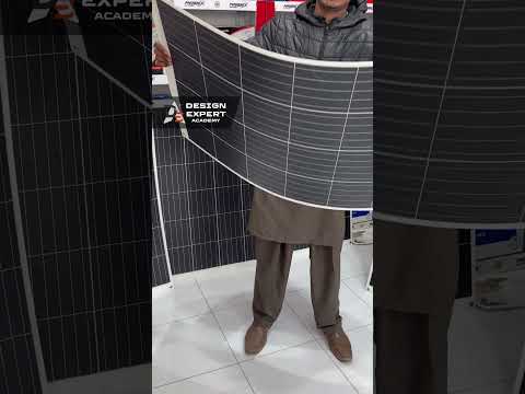
- Flexibility and Lightweight Design: Thin-film PV’s unique form factors enable integration into non-traditional surfaces, such as curved building facades, vehicles, and portable electronics, expanding addressable markets.
- Supply Chain Diversification: Thin-film technologies rely less on polysilicon, mitigating risks associated with silicon supply constraints and price volatility.
Regionally, Asia-Pacific remains the largest market, driven by large-scale solar deployments in China and India, while North America and Europe are witnessing increased adoption in niche applications and distributed generation (International Energy Agency). Key players in the sector include First Solar, AVANCIS, and Solar Frontier, each investing heavily in next-generation thin-film technologies.
In summary, thin-film photovoltaic engineering is poised for robust growth in 2025, supported by technological advancements, cost reductions, and expanding application areas. The sector’s evolution will be shaped by continued innovation, policy support for renewables, and the ability to address emerging energy needs in both developed and developing markets.
Key Technology Trends in Thin-Film Photovoltaics
Thin-film photovoltaic (PV) engineering in 2025 is characterized by rapid advancements in materials science, device architecture, and manufacturing processes, all aimed at improving efficiency, reducing costs, and expanding application versatility. The sector is witnessing a shift from traditional amorphous silicon (a-Si) to more efficient compounds such as cadmium telluride (CdTe), copper indium gallium selenide (CIGS), and emerging perovskite-based thin films.
One of the most significant trends is the integration of tandem and multi-junction architectures, where thin-film layers are stacked to capture a broader spectrum of sunlight. This approach has enabled laboratory-scale devices to surpass 25% efficiency, narrowing the gap with crystalline silicon and making thin-film PV more competitive for utility-scale and distributed generation projects. Notably, perovskite/silicon tandem cells have demonstrated rapid efficiency gains, with several pilot lines targeting commercial viability by 2025 National Renewable Energy Laboratory.
Manufacturing innovations are also central to thin-film PV engineering trends. Roll-to-roll processing, inkjet printing, and other scalable deposition techniques are reducing production costs and enabling flexible, lightweight modules. These advances are particularly relevant for building-integrated photovoltaics (BIPV) and portable power applications, where form factor and weight are critical considerations International Energy Agency.
Material sustainability and supply chain resilience are gaining prominence. Efforts to reduce or eliminate toxic elements (such as cadmium in CdTe) and reliance on scarce materials (like indium and tellurium) are driving research into alternative compounds and recycling processes. For example, the development of earth-abundant kesterite (CZTS) and all-inorganic perovskite materials is being actively pursued to address these concerns Helmholtz-Zentrum Berlin.
Finally, digitalization and advanced monitoring are being integrated into thin-film PV engineering. Smart manufacturing, real-time quality control, and predictive maintenance are enabled by AI and IoT technologies, improving yield and module reliability. These trends are expected to accelerate the commercialization of next-generation thin-film PV products and expand their adoption across diverse markets in 2025 and beyond Wood Mackenzie.
Competitive Landscape and Leading Players
The competitive landscape of thin-film photovoltaic (PV) engineering in 2025 is characterized by a dynamic mix of established multinational corporations, innovative startups, and research-driven partnerships. The sector is marked by rapid technological advancements, cost-reduction strategies, and a growing emphasis on sustainability and scalability. Thin-film PV technologies—primarily cadmium telluride (CdTe), copper indium gallium selenide (CIGS), and amorphous silicon (a-Si)—are increasingly competing with traditional crystalline silicon modules, particularly in applications where flexibility, lightweight, and low-light performance are critical.
Leading Players
- First Solar, Inc.: As the global leader in CdTe thin-film modules, First Solar continues to dominate the market with its vertically integrated manufacturing and significant investments in R&D. The company’s Series 6 and Series 7 modules have set industry benchmarks for efficiency and cost per watt, and its expansion into new gigawatt-scale factories in the U.S. and India underscores its commitment to scaling production and meeting global demand.
- Hanwha Q CELLS: While primarily known for crystalline silicon, Hanwha Q CELLS has invested in CIGS thin-film technology through its subsidiary, Hanwha Solutions. The company leverages advanced engineering to improve module efficiency and durability, targeting both utility-scale and building-integrated PV (BIPV) markets.
- Solar Frontier K.K.: A pioneer in CIGS technology, Solar Frontier has maintained a strong presence in Asia and Europe. Its proprietary CIS modules are recognized for high performance in real-world conditions, particularly under low-light and high-temperature environments.
- OXIS Energy: Although primarily focused on battery technology, OXIS Energy has entered the thin-film PV space through collaborative projects, aiming to integrate lightweight solar solutions with energy storage for off-grid and mobile applications.
- Heliatek GmbH: Specializing in organic photovoltaic (OPV) thin films, Heliatek is at the forefront of flexible, ultra-lightweight solar solutions. Its HeliaSol and HeliaFilm products are gaining traction in BIPV and niche applications where traditional modules are unsuitable.
Strategic partnerships, intellectual property portfolios, and manufacturing scale are key differentiators among leading players. The competitive environment is further shaped by government incentives, trade policies, and the ongoing push for higher module efficiencies and lower levelized cost of electricity (LCOE). As the market matures, consolidation and collaboration are expected to intensify, with innovation in materials science and process engineering remaining central to competitive advantage in thin-film PV engineering.
Market Growth Forecasts (2025–2030): CAGR, Revenue, and Volume Analysis
The thin-film photovoltaic (PV) engineering market is poised for robust growth between 2025 and 2030, driven by technological advancements, declining production costs, and increasing global demand for renewable energy. According to projections by MarketsandMarkets, the global thin-film solar cell market is expected to register a compound annual growth rate (CAGR) of approximately 8.5% during this period. This growth is underpinned by the rising adoption of thin-film PV technologies in utility-scale solar farms, building-integrated photovoltaics (BIPV), and portable power applications.
Revenue forecasts indicate that the market could surpass USD 25 billion by 2030, up from an estimated USD 15 billion in 2025. This expansion is attributed to the increasing efficiency of thin-film modules, particularly those based on cadmium telluride (CdTe) and copper indium gallium selenide (CIGS) technologies, which are gaining traction due to their lower material costs and flexibility compared to traditional crystalline silicon panels. International Energy Agency (IEA) data highlights that thin-film PV is expected to account for a growing share of new solar installations, especially in regions with high temperature variability and limited rooftop load capacity.
Volume analysis reveals that annual thin-film PV module shipments are projected to reach over 30 GW by 2030, up from approximately 18 GW in 2025. This surge is fueled by large-scale investments in manufacturing capacity, particularly in Asia-Pacific, where countries like China and India are ramping up production to meet both domestic and export demand. Wood Mackenzie reports that thin-film technologies are increasingly favored for utility-scale projects due to their superior performance in low-light and high-temperature environments.
- CAGR (2025–2030): ~8.5%
- Projected Revenue (2030): USD 25+ billion
- Projected Volume (2030): 30+ GW annual shipments
Overall, the thin-film photovoltaic engineering sector is set for significant expansion, with innovation, cost competitiveness, and supportive policy frameworks acting as key growth drivers through 2030.
Regional Market Analysis: North America, Europe, Asia-Pacific, and Rest of World
The thin-film photovoltaic (PV) engineering market demonstrates distinct regional dynamics across North America, Europe, Asia-Pacific, and the Rest of the World, shaped by policy frameworks, investment trends, and technological adoption.
North America remains a significant player, driven by robust investments in renewable energy and supportive government policies. The United States, in particular, has seen increased deployment of thin-film PV in utility-scale and commercial projects, spurred by the Inflation Reduction Act and state-level renewable portfolio standards. Companies such as First Solar continue to expand manufacturing capacity, leveraging cadmium telluride (CdTe) technology. The region’s focus on domestic supply chains and energy security is expected to further boost thin-film PV engineering through 2025.
Europe is characterized by aggressive decarbonization targets and a strong emphasis on sustainability. The European Union’s Green Deal and REPowerEU initiatives have accelerated the adoption of thin-film PV, particularly in building-integrated photovoltaics (BIPV) and urban infrastructure. Leading players like Heliatek and OXIS Energy (for research collaborations) are advancing organic and perovskite-based thin-film solutions. The region’s focus on circular economy principles and recycling is also influencing engineering approaches, with increased R&D in eco-friendly materials and end-of-life management.
- Asia-Pacific dominates global thin-film PV production, led by China, Japan, and South Korea. China’s government-backed initiatives and the presence of major manufacturers such as Hanergy have resulted in large-scale deployment and cost reductions. Japan’s focus on high-efficiency, flexible thin-film modules for residential and commercial rooftops, and South Korea’s investments in next-generation CIGS (copper indium gallium selenide) technology, are shaping regional engineering trends. The Asia-Pacific market is expected to maintain its leadership in both innovation and volume through 2025.
- Rest of World markets, including Latin America, the Middle East, and Africa, are emerging as new frontiers for thin-film PV engineering. These regions benefit from high solar irradiance and growing energy demand. Projects in countries like the United Arab Emirates and Chile are increasingly incorporating thin-film PV for utility-scale solar farms, supported by international financing and technology transfer from established players.
Overall, regional market analysis reveals that while Asia-Pacific leads in manufacturing and deployment, North America and Europe are driving innovation and sustainability in thin-film photovoltaic engineering. The Rest of World segment is poised for rapid growth as technology costs decline and energy access initiatives expand.
Future Outlook: Emerging Applications and Investment Hotspots
Looking ahead to 2025, thin-film photovoltaic (PV) engineering is poised for significant transformation, driven by both technological innovation and shifting investment priorities. The sector is expected to benefit from the convergence of advanced materials science, manufacturing scalability, and the global push for decarbonization. As traditional silicon-based PV technologies approach their theoretical efficiency limits, thin-film PV—encompassing cadmium telluride (CdTe), copper indium gallium selenide (CIGS), and perovskite materials—offers new pathways for cost reduction, flexibility, and integration into diverse applications.
Emerging applications are a key driver of future growth. Building-integrated photovoltaics (BIPV) are gaining traction, with thin-film modules being favored for their lightweight, flexible, and semi-transparent properties, making them ideal for facades, windows, and roofing in urban environments. The transportation sector is another hotspot, as thin-film PV is increasingly integrated into electric vehicles, trains, and even drones, providing auxiliary power and extending operational range. Additionally, the rise of the Internet of Things (IoT) and off-grid electronics is fueling demand for thin-film PV in portable and wearable devices, where form factor and weight are critical considerations.
From an investment perspective, Asia-Pacific remains the dominant region, with China and Japan leading in both manufacturing capacity and deployment. However, Europe and North America are emerging as innovation hubs, particularly in perovskite research and BIPV commercialization. Venture capital and corporate investments are increasingly targeting startups focused on tandem cell architectures and roll-to-roll manufacturing, which promise to further lower costs and improve efficiency. According to International Energy Agency projections, thin-film PV could account for up to 20% of new solar installations by 2030, with perovskite-based modules expected to enter commercial production at scale by 2025.
- Key investment hotspots include perovskite-silicon tandem cells, flexible and transparent PV modules, and advanced encapsulation technologies to improve durability.
- Strategic partnerships between material suppliers, module manufacturers, and construction firms are accelerating BIPV adoption.
- Government incentives in the EU and US, such as the Inflation Reduction Act, are catalyzing domestic thin-film manufacturing and R&D.
In summary, 2025 will mark a pivotal year for thin-film photovoltaic engineering, with emerging applications and targeted investments reshaping the competitive landscape and unlocking new market opportunities.
Challenges, Risks, and Strategic Opportunities
Thin-film photovoltaic (PV) engineering faces a complex landscape of challenges and risks in 2025, but these are counterbalanced by significant strategic opportunities. The sector’s primary technical challenge remains the efficiency gap between thin-film technologies—such as cadmium telluride (CdTe), copper indium gallium selenide (CIGS), and emerging perovskites—and conventional crystalline silicon PV. While thin-film modules offer advantages in flexibility, weight, and potential for lower manufacturing costs, their average conversion efficiencies still lag behind mainstream silicon, which can impact large-scale adoption and investor confidence (National Renewable Energy Laboratory).
Material supply chain risks are also prominent. Thin-film PV relies on critical raw materials like indium, tellurium, and gallium, which are subject to geopolitical supply constraints and price volatility. For example, the limited availability of tellurium and indium has led to concerns about the scalability of CdTe and CIGS technologies (International Energy Agency). Additionally, the environmental and health risks associated with cadmium use in CdTe modules pose regulatory and public perception challenges, particularly in regions with stringent environmental standards.
From a manufacturing perspective, thin-film PV production requires high capital investment in specialized equipment and process optimization. Yield losses, process uniformity, and long-term module stability remain engineering hurdles, especially for newer materials like perovskites, which are susceptible to moisture and UV degradation (pv magazine).
Despite these challenges, strategic opportunities abound. The lightweight and flexible nature of thin-film PV enables integration into building materials (BIPV), vehicles, and portable devices—markets less accessible to rigid silicon panels. The rapid progress in perovskite tandem cells, which can be layered atop silicon or other thin-film materials, offers a pathway to surpass current efficiency records and reduce levelized cost of electricity (LCOE) (Wood Mackenzie).
- Strategic partnerships between thin-film innovators and established construction or automotive firms can accelerate market penetration.
- Investment in recycling and circular economy solutions for thin-film modules can mitigate material supply risks and address end-of-life concerns.
- Government incentives and targeted R&D funding, especially in the US, EU, and China, are expected to drive commercialization and scale-up efforts in 2025 (International Energy Agency).
In summary, while thin-film PV engineering in 2025 must navigate efficiency, supply chain, and regulatory risks, the sector’s unique attributes and ongoing innovation position it for strategic growth in emerging and specialized solar markets.
Sources & References
- MarketsandMarkets
- First Solar
- International Energy Agency
- AVANCIS
- Solar Frontier
- National Renewable Energy Laboratory
- Helmholtz-Zentrum Berlin
- Wood Mackenzie
- Heliatek GmbH